Engineered for 5G communication and industrial control, our bare boards ensure maximum reliability. As a premier pcba manufacturer, we deliver scalable layout configurations designed to streamline your assembly workflows.
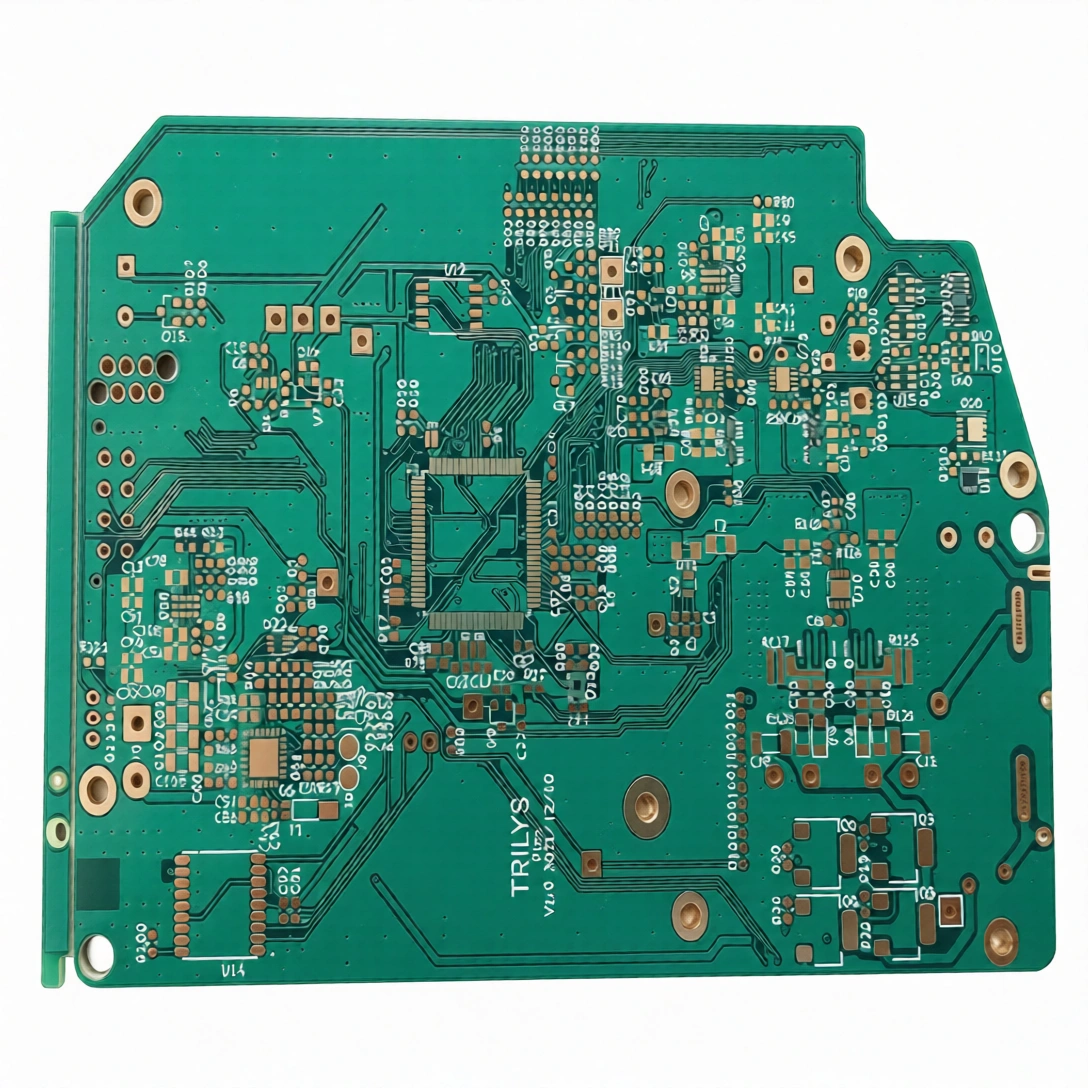
Supporting complex 1 to 36 layer stack-ups. Precision lamination techniques ensure structural integrity under extreme thermal cycling.
Strict ±10% tolerance control for high-speed signal routing, critical for next-generation telecommunications and data centers.
End-to-end material procurement and capacity scaling designed specifically to support major EMS and OEM production lines.
Engineered for strict tolerances, our boards scale from 1 to 36 layers for rigid and flex needs. Optimized for intricate routing and HDI architectures, they ensure minimal signal loss. Built by premier pcb assembly manufacturers, they streamline prototyping to mass production with stringent QA.
| Layer Count | 1 – 36 Layers (Rigid, Flex, Rigid-Flex) |
|---|---|
| Material Options | FR4, Rogers, PTFE, Polyimide, Metal Core |
| Min. Line/Space | 3 mil / 3 mil (HDI capabilities available) |
| Surface Finishes | ENIG, HASL Lead-Free, Immersion Silver/Tin, OSP |
Production Strategy
Capabilities
Innovation
Trusted by engineering teams and procurement officers globally.
"The impedance control on their 12-layer HDI boards is exceptional. As an OEM, finding a manufacturer that scales seamlessly from our initial engineering runs to full 10K+ batch orders without any drop in yield has been critical."
"Their heavy copper capability and thermal management properties have significantly reduced our field failure rates. Consistent quality and reliable delivery timelines make them a top-tier supply chain partner."
"A highly professional manufacturing partner. The 100% AOI testing ensures we receive pristine boards ready for immediate SMT processing, severely cutting down our own QA overhead."
We support scalable manufacturing. While prototypes can be produced in low quantities, our volume production pricing offers competitive tiered discounts starting from 500 square meters.
Upon final Gerber file verification, standard mass production lead times range from 12 to 18 business days depending on layer count and specific HDI requirements.
Yes, our facilities operate under strict ISO9001 and IATF16949 quality management systems, and all boards are UL certified and RoHS compliant.
We utilize advanced calculation models and precise etching techniques to maintain ±10% or better impedance tolerance, providing TDR test reports with every shipment.
Absolutely. We are fully equipped to handle complex HDI architectures, including multi-tier blind/buried vias, VIPPO (via-in-pad plated over), and heavy copper up to 6oz.
We implement a 100% AOI (Automated Optical Inspection) and flying probe/fixture electrical testing protocol to eliminate open/short circuits prior to assembly.
